
Mobile Phone Charging Problems: A Practical Diagnostic Guide
02 May 2025
S.A. Syal Suleman
8 MIN READ
SHARE PROTOCOL
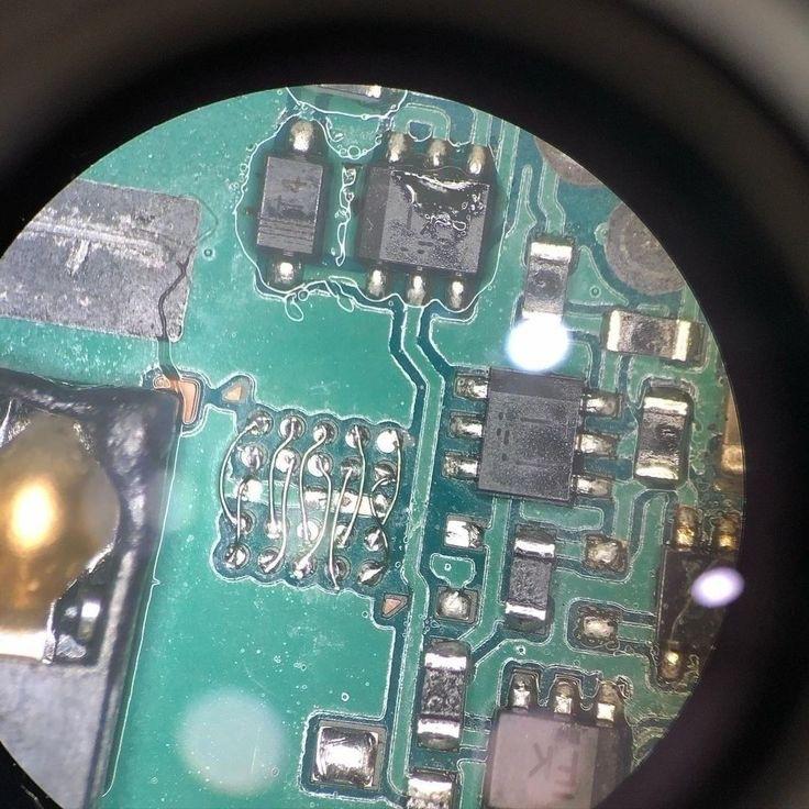
Charging anomalies account for a significant percentage of mobile hardware repairs. Modern USB Type-C and Power Delivery (PD) architectures require a structured approach to differentiate mechanical port wear from active semiconductor failures.
1. Mechanical Port & CC Line Diagnostics Before condemning board-level components, inspect the USB Type-C connector under high optical magnification. - Verify structural integrity of CC1 and CC2 (Configuration Channel) pins. If CC lines are open, the charger cannot negotiate fast charging voltages (9V/12V). - Test VBUS pin continuity from port to board sub-flex connector.
2. Over-Voltage Protection (OVP) Circuit Testing The OVP chip shields internal power ICs from voltage spikes. - Measure VBUS input voltage at the input capacitor of the OVP (typically 5.0V to 9.0V). - Measure VBUS output at the downstream capacitor. If input voltage is present but output is 0V, the OVP gate driver is either damaged or latched in protection mode.
3. Charging IC & Fuel Gauge Communication Modern Android devices rely on dedicated charging management ICs (e.g., SMB series or integrated PMIC blocks) communicating with the fuel gauge via I2C/SMBus. - Verify the presence of the BATSNS and NTC thermistor line voltages (approx. 1.8V). - If thermal resistance readings deviate, the device will flag fake charging or display temperature warning alerts.
Understanding the entire current pathway prevents unnecessary component swapping.
Topical Reference Tags
#charging#type-c#ovp#battery-ic#hardware